We have seen how we can construct small memories out of flip flops. To build larger memories, we can essentially bundle a lot of flip flops together. Today we will look at some facets of these larger memory systems.
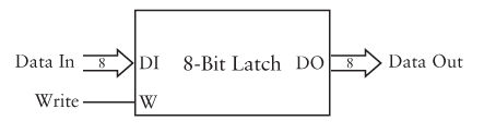
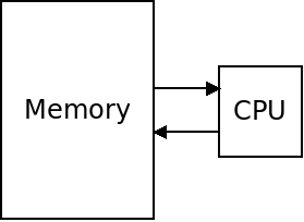
In a recent lab, we built an 8-bit register out of 8 flip flops. The register could store and recall an 8-bit value and could be drawn schematically like this (a latch is another name for a register):
We could also have designed it so that it can recall the individual bits separately using a 3-bit input to select which one we want:
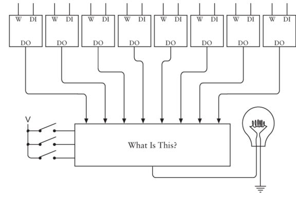
The "What Is This?" logic is described in Code as an "8-to-1 Selector", but is more usually called a "Multiplexer". Its job is to choose which of a set of inputs to pass along as output using a value to select which one is used. You can think of it as the hardware version of a "switch" statement.
How could we build the multiplexer?
If we wanted the ability to write the various bits individually, we could do so in a similar manner:
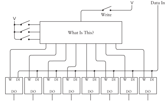
Here the "What Is This?" logic is a "Decoder", which we have seen before. It's job is to take the 3-bit signal and decode it into 8 1-bit signals such that each one is only set when the 3-bit value refers to it.
How could we build the decoder?
We can combine these two circuits so that we can read or write any of the bits:
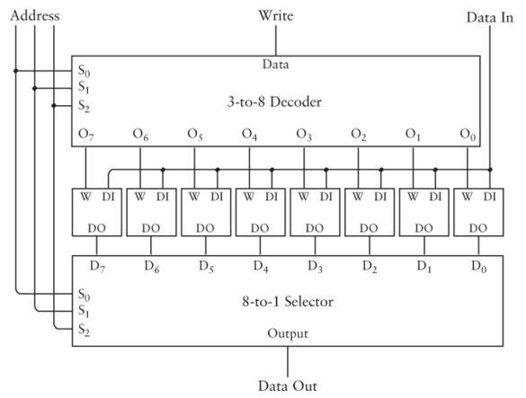
This circuit is essentially a small RAM where each value is just one bit, and there are 8 of them. We can change the 8 flip flops to be larger registers to get a RAM of 8 larger values.
We can also increase the number of values. When we increase the number of values, it makes sense to double them. This is because we would need more address bits to address more memory. If we add a fourth one, then we would be able to access 16 values. If we add a fifth, we would have 32 values, and so on.
Unfortunately, this doesn't scale perfectly. If we want a 1 gigabyte RAM, we would need $2^{30}$ bytes values, which would be selected with a 30-bit address line. It is just not practical to build a "30 to $2^{30}$" multiplexer.
Instead, we need to arrange the memory into "banks". This means it would be internally divided into smaller, independent memories. To access a bit, we would use some part of the address to select which memory bank, and the rest to address inside of the bank. This makes the memory slower, but avoids needing huge multiplexers.
For this reason, it is impossible to make memories which are both really big and really fast. The larger we choose to make a memory, the slower it will be. This is also partly due to the larger memory chips just taking more time for signals to propagate.
Because we can't have one large, fast memory, we instead have a hierarchy of memory, with some small fast memories and some large slow ones.
The following table gives common levels of the memory hierarchy, along with estimate values of the sizes and times. Exact values depend on the architecture, but these give you an idea:
| Memory | Size | Latency |
| Register File | Tiny (1 Kb) | 1 clock cycle |
| Level 1 Cache | Small (32 Kb) | 2 clock cycles |
| Level 2 Cache | Medium (4 Mb) | 8 clock cycles |
| Main Memory | Large (8 Gb) | 200 clock cycles |
| Hard Drive | Huge (1 Tb) | 10,000,000 clock cycles |
The register file is the smallest addressable memory inside of a processor. It is used for values the CPU operates on directly. The compiler (or assembly programmer) is responsible for putting values into or out of the register file.
As we will discuss below, caches are used to store a portion of main memory to make it faster to access.
Hard drives are not really part of the memory system, and they work totally differently, but as you can see, they are much slower than the memories we are discussing.
We have talked about the GBA memory system indirectly, but here we will see the complete memory system. It is actually composed of several different memories which share one address space:
| Start Address | End Address | Size | Description |
| 0x0000:0000 | 0x0000:3fff | 16 kb | BIOS memory. |
| 0x0200:0000 | 0x0203:ffff | 256 kb | External work memory (larger and slower). |
| 0x0300:0000 | 0x0300:7fff | 32 kb | Internal work memory (smaller and faster). |
| 0x0400:0000 | 0x0400:03ff | 1 kb | Hardware control registers. |
| 0x0500:0000 | 0x0500:03ff | 1 kb | Palette memory. |
| 0x0600:0000 | 0x0601:7fff | 96 kb | Video RAM. |
| 0x0700:0000 | 0x0700:03ff | 1 kb | Sprite memory. |
| 0x0800:0000 | - | Variable | Game Pak ROM (executable code and data of the game). |
| 0x0e00:0000 | - | Variable | Cart RAM (save game data). |
Notice that the end of one section does not match up with the start of the next. This means some memory addresses are invalid and don't refer to any real memory on the GBA.
The GBA does not have a cache, but it does have the external work RAM (EWRAM) and internal work RAM (IWRAM) sections which function somewhat like a cache, except it the programmer or compiler's job to manage them.
We have been relying on the compiler to handle this for us, but by programming in assembly, we can decide if our code and data should go in the smaller, faster, IWRAM.
Normally when memory is accessed, it is done through the CPU. This is usually not a problem because the CPU usually processes the data which is accessed directly.
There are some cases, however, where this is not optimal. For instance, if we are copying a block of memory from one address to another, it is not efficient to rout it through the CPU.
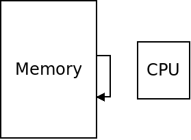
Instead, we can use direct memory access (DMA) in which memory transfers happen outside of the CPU. With DMA, blocks of memory can be transferred directly from one part of memory to another:
DMA can also be used to transfer data from memory to an I/O device such as a graphics card or hard drive.
DMA is normally handled by the operating system and device driver software. On the GBA, however, there is no operating system or drivers.
We can use DMA on the GBA, but we have to do it ourselves. To do so, there are a few more hardware registers:
/* pointer to the DMA source location */
volatile unsigned int* dma_source = (volatile unsigned int*) 0x40000D4;

/* pointer to the DMA destination location */
volatile unsigned int* dma_destination = (volatile unsigned int*) 0x40000D8;

/* pointer to the DMA count/control */
volatile unsigned int* dma_count = (volatile unsigned int*) 0x40000DC;
The dma_source register stores the source of the DMA transfer, the dma_destination stores the destination. To turn on a DMA transfer, we store pointers to the source and destination in these two registers.
The dma_count register stores both the number of values to transfer and control signals detailing how the transfer should work. The lowest 16 bits are the size. The highest bit is the enable bit. When 0, no DMA takes place. When 1, a DMA is triggered.
The 26th bit is also important, it determines the size of transfers. If 0, it's 16-bit values, and if 1, it's 32 bit ones. The following defines can be used to set these values:
/* flag for turning on DMA */
#define DMA_ENABLE 0x80000000

/* flags for the sizes to transfer, 16 or 32 bits */
#define DMA_16 0x00000000
#define DMA_32 0x04000000
There are several other control values which allow more fine-grained control.
Without DMA, we would write a function to transfer memory from one location to another with a loop:
/* copy data with a loop */
void memcpy16(unsigned short* dest, unsigned short* source, int amount) {
    for (int i = 0; i < amount; i++) {
        dest[i] = source[i];
    }
}
We can do the same thing but faster using DMA instead:
/* copy data using DMA */
void memcpy16_dma(unsigned short* dest, unsigned short* source, int amount) {
    *dma_source = (unsigned int) source;
    *dma_destination = (unsigned int) dest;
    *dma_count = amount | DMA_16 | DMA_ENABLE;
}
This code stores the source and destination locations in the hardware registers, and then combines the amount with the flags for 16 bits, and the enable bit. This suspends the CPU until the memory transfer has finished.
This program tests the loop-based copy and the DMA-based one. It contains both memory copy functions above and calls one of them a number of times. The DMA one runs far faster.
Copyright © 2024 Ian Finlayson | Licensed under a Attribution-NonCommercial 4.0 International License.