Sequential Logic
Overview
We've made lots of things that compute, but how do we create a memory? How can we store information inside of a circuit?
All of the circuits we've made so far are "combinational" which means that the output is a function of the inputs only. Changing the inputs will change the output, and the circuit has no ability to "remember" anything.
Combinational circuits follow this pattern:
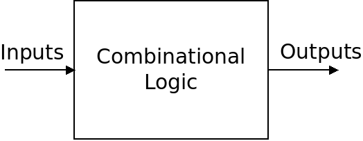
We can change the behavior of the circuit by changing the gates inside of the circuit, but the output changes in response to the inputs without any history.
Sequential Logic
Sequential logic is another type of logic where circuits do have the ability to remember. They do this by feeding the outputs back into the inputs of the circuit:
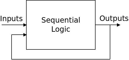
Because the outputs cycle back to the inputs, it is possible for sequential circuits to have history. They can take their past outputs into account when computing their new outputs.
Sequential circuits form the basis of all computer memories, but are more complex than combinational circuits.
Flip Flops
A "flip flop" is a circuit which can be used to store a single bit. It is called this because it can switch between the two states, 0 and 1. The simplest flip flop is the "SR" flip flop which is pictured below:
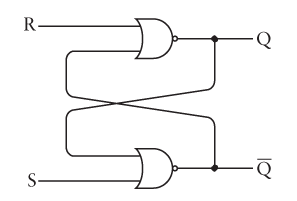
The circuit has two input pins, $S$ which stands for set, and $R$ which stands for reset. It has two outputs $Q$ and $\overline{Q}$ which reflect the value of the flip flop and its complement.
Notice that the outputs cycle back to the inputs of the flip flop which makes it sequential. What is the truth table of this circuit?
D Flip Flops
The SR flip flop is simple, but if we are building a memory, it's not convenient to have to set the S and R to 1 for a 1 or 0 independently. The D type flip flop takes to inputs instead: "Data" which is the value to store, and "Clock" which controls setting the flip flop. When clock is 0, the flip flop is unchanged, and when it is 1, the value of "Data" is stored:
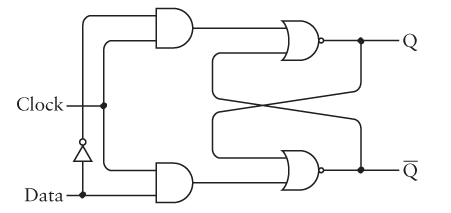
Notice that this is just a minor extension of the SR flip flop above. We just have a little extra logic to decide when to "Set" and when to "Reset".
What is the truth table of this circuit?
Clocks
The input which controls the flip flop is labeled "Clock" because it is used to synchronize the flip flop with the rest of the hardware. A computer system has lots of different memories and control signals and we need to keep them synchronized with each other.
The clock in a processor is a single signal which is sent to all logic components that need it. The "clock speed" is the frequency at which the clock signal switches between 0 and 1.
Level Triggering vs. Edge Triggering
In the circuit above, we store the value of Data into the flip flop whenever the Clock is 1. This is called "Level Triggering" because the flip flop is triggered by the level of the clock: either 0 or 1.
There is an issue with level triggering, however, which is that when the clock is 1, any changes to Data will affect the flip flop. This makes it harder to make fast circuits that stay in lock step because there is a wide period of time (whenever Clock is 1) where we cannot change Data.
Instead, we can use "Edge Triggering" which means that the flip flop only stores its value when the clock changes from one value to another. Usually we use the change from 0 to 1 which is called the "Rising Edge".
An edge-triggered D-type flip flop is shown below:
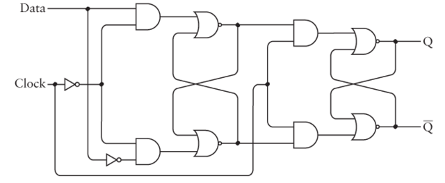
Note that it is essentially two level-triggered flip flops joined together. The clock controls both halves of the flip flop, but it is inverted for the first half. This means that when the clock is 0, Data will propagate through the first half. But it will not propagate through the second half until the clock is 1.
The net result is that only when the clock changes from 0 to 1 will the Data value be set as $Q$. After it is on 1, the Data value won't get through the first half any more.
Adding a Reset Switch
Oftentimes flip-flop circuits will include an asynchronous reset input. Here "asynchronous" means that the reset will bypass the clock and reset the flip-flop to 0 regardless of the clock's value.
This is helpful when we want to ensure that the flip-flop is in some predictable state to begin with.
This can be easily accomplished by connecting the reset signal into an OR gate with the output of the topmost AND. Recall that the top-right NOR gate was our original "reset" input in the first "SR" flip-flop which we looked at.
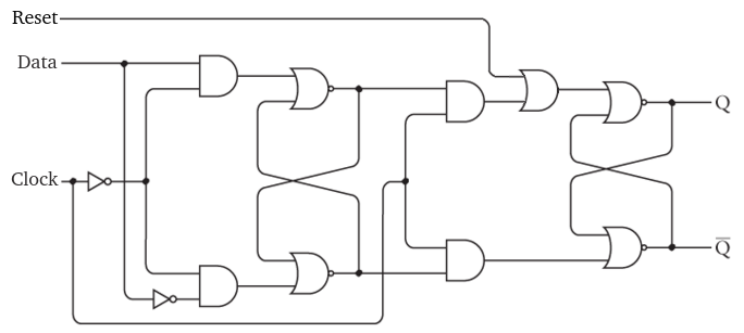
When the reset is 1, the flip-flop will reset to 0 regardless of the other inputs.